Recently I’ve been expanding my retro game collection to include game cartridges imported from Japan. The problem is that I don’t have Japanese game systems (yet). So I’m creating an open source adapter to convert Famicom carts to the NES. Before I submit the PCB to OSH Park, I’m going to run through this PCB Checklist to make sure I don’t forget something silly.
This PCB checklist is something I’ve built over my years of creating boards. If you’ve got tips from your own list, don’t forget to leave a comment letting us know.
PCB Production Checklist
The concepts on this list will apply to almost any PCB software. The tips I give relate to EAGLE, since that is what I use most often. Feel free to comment to add tips for other design software like upverter.com or KiCad.
Make sure you also check out the comments, some really great suggestions there too!
1. Dimension Outline
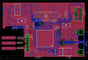
After your board is done processing, a CNC router will cut the panel. The router uses the dimension layer to run the cutting bit. So make sure the shape of the dimension layer is what you want. Most board services will let you cut almost any shape (but charge you as if the board fit inside of a quadrilateral.)
The example above, you can see I made a cut-out for the Wii’s accessory connector. Not all (cheap) services allow cuts inside your design, so double-check before you send it out.
2. Mounting Holes
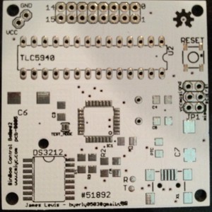
One of the biggest mistakes I make with every PCB, is to forget mounting holes. I get so caught up in part placement, I forget to consider how I’m going to mount the board into a case. At the very least, make sure you add some holes to the board’s design.
The example here is from my Binary Clock controller. Notice right above the RTC (DS3212) that there is a small hole. That’s because when I got the first board back, I realized the battery was on the bottom layer and had no way to push the battery out from behind! So that hole lets me stick a small screwdriver inside to push out the battery.
3. Clearance for Connectors
This check list item requires a bit of experience or a lot of 3D CAD work.
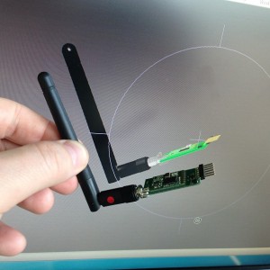
BinBoo is one of my favorite projects. It was my first experience with a laser cutter and one of my first PCBs to run through my toaster reflow oven. However, I have to keep the back panel off, because the USB connector isn’t offset enough. I lined up the edge of the connector’s layout with the edge of my PCB’s dimension layer. I should have extended the connector off the edge a little, so that it had enough clearance to get past the back panel.
4. Component Labels
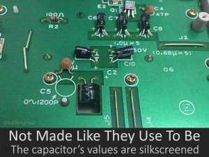
Even though leaving off part values could be a quick short cut, it can make board assembly a little more frustrating. Make sure each part (especially the passive components like resistors, capacitors, and inductors) have a value associated with them. Once you’ve added those, carefully look each part to make sure both the designated (R1, R3, etc) and the value are in a place that makes sense.
EAGLE Tip: Use SMASH
The SMASH Command in EAGLE will separate the NAME and VALUE labels from a part. This will let you move them anywhere. This is really useful for when you have parts overlapping or the silkscreen is “off the board.”
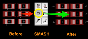
Nothing is worse than getting a board back and getting confused about whether you should be placing a 100ohm or 1000ohm resistor.
5. Label Important (All) Pins — Both Sides
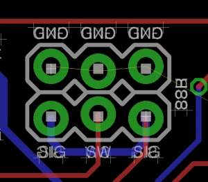
This is especially helpful on boards with through-hole parts. Put a mirrored label on the bottom side of the board. This way when you have it flipped over, you can easily find where different components are. Otherwise, you’ll end up flipping the board over a few times (or try to turn your head upside down) to find your place.
EAGLE Tip: Use Layers 25 tNames and 26 bNames for pin labels. If you select 26 bNames before creating the label, EAGLE will automatically mirror the text for you.
6. Print out a 1:1 Copy
Print the board design on a piece of paper, and place components on the paper. If you have some foam, you can even put some through-hole parts down as well. Then move around with a pencil tip and see if your soldering iron is going to hit something plastic by example.
7. Add a revision number and your name
Sometimes a board will come back with a mistake on it. Sometimes that mistake is so bad you have to send it out again (or “re-spin” it.) In those cases, you might end up with two boards floating around your workbench that look very similar. Adding a “rev 1” tag to one side of the board will help you find which version you have, even if you think you’ll only make one.
Don’t forget to add some text with your name and/or the name of the board. I like to put this on both sides of the board.
Bonus Tip: Include the OSH Logo (if your project is OSH…) The Adafruit EAGLE libraries include one.
8. Double check the final files
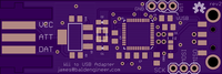
One of the cool features of OSH Park’s PCB service is that you’ll see a rendered version of your board’s EAGLE files. If you are submitting gerber files, there are free Gerber viewers that let you see a graphical versions of the gerber files.
Make sure they make sense before you send. Double check that traces aren’t overlapping, that traces don’t touch vias or through-holes, and that ground planes aren’t shorting anything out.
Speaking of ground planes…
9. Don’t forget Ground Planes
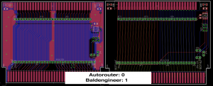
When you first start making PCBs, you might notice a slight difference between your boards and other people’s boards. Good PCBs always include some ground (and sometimes power) planes in the empty spaces.
To make these is actually pretty simple, at least in EAGLE. Draw polygons on both layers of your board, name them GND, and connect them together with some Vias. These ground planes will help provide better signal integrity with a lower impedance path to ground. Use this video tutorial on creating ground planes in EAGLE to learn more. (Hint: there is a trick in there.)
This is my checklist for submitting a PCB to a fab house. What are your last minute must-do items or gotchas?